Resources
Highlights
Introduction
In this project, I implemented a digital circuit capable of performing a common image-processing task: combining adjacent pixels with different weights.
Implementation
The work began with an exploration of potential applications and architectural options for the circuit. Then, the circuit was designed and implemented using VHDL, employing a bottom-up approach, i.e., creating basic building blocks (e.g., flip-flops, adders, counters, …) and progressively integrating them to construct a more complex circuit.
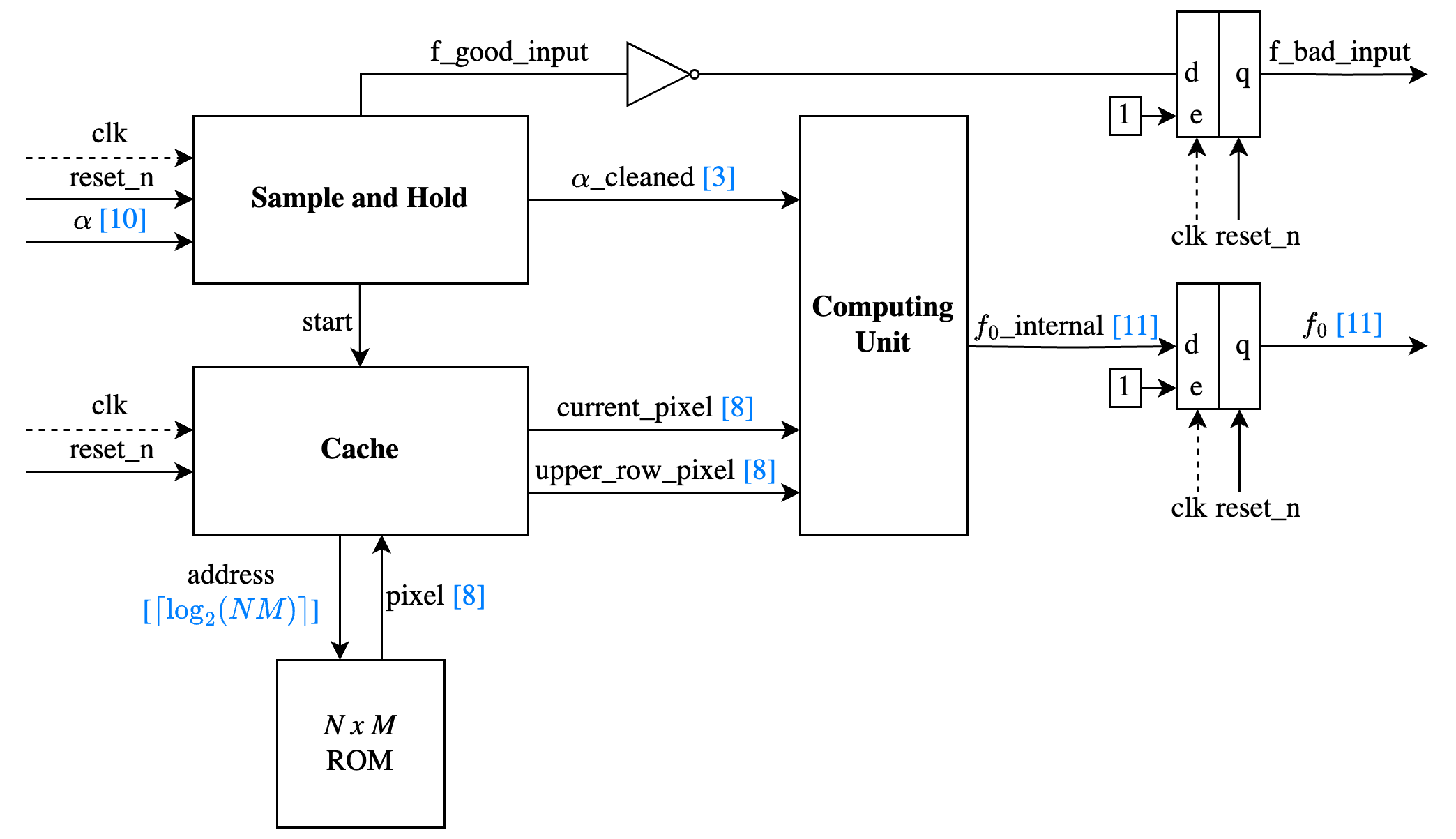
Block diagram of the implemented circuit
Verification
Once the design was completed, the circuit was validated through the analysis of the simulated waveforms of every component (done using ModelSim-Intel© FPGAs Standard Edition 2020.1).
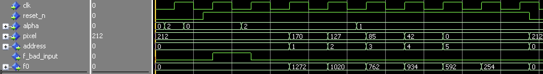
Waveform of the input and output ports of the circuit using a simple 2x3 test ROM
Moreover, the circuit was tested using real images. This was achieved by:
- Converting the selected image into a VHDL ROM
- Simulating the circuit
- Exporting the waveform of the output port
- Parsing the pixels and constructing the output image

Input image (3-3-2 bitmap)

Output image (3-3-2 bitmap, α = 0.500)

Input image (grayscale)

Output image (grayscale, α = 0.500)
Synthesis
Finally, the circuit was synthesized using Vivado 2024.1, and its timing, power consumption, and resource utilization statistics were analyzed, also considering slightly different variations of the circuit’s parameters (e.g., ROM size, precision of α, number of bits per pixel, …).
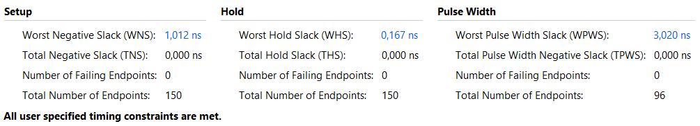
Timings
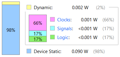
Power consumption
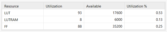
Resource utilization